
As electronics become more compact, powerful, and sophisticated, PCB design faces increasing challenges. Two essential elements that define the functionality and performance of modern printed circuit boards are the copper trace and SOIC package. Their correct integration is key to building efficient, reliable, and scalable electronic products.
What Is a Copper Trace?
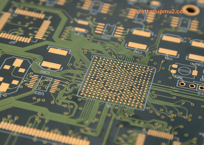
A copper trace is the conductive pathway on a PCB that carries electrical signals and power between components. It is essentially the “wiring” within the board, replacing traditional wires with thin layers of copper etched onto the board’s surface.
Copper trace design requires careful planning of several factors:
- Trace width, determined by the amount of current the trace needs to carry
- Trace thickness, commonly specified as 1 oz, 2 oz, or more per square foot
- Routing paths to minimize electromagnetic interference and signal loss
- Spacing between traces to prevent short circuits
Using advanced PCB trace calculators, designers calculate the optimal width and thickness to ensure that the copper trace can safely handle electrical loads without overheating or introducing excessive resistance.
Understanding the SOIC Package
The SOIC package, or Small Outline Integrated Circuit, is a widely used surface-mount component package. Unlike through-hole packages, SOIC allows components to sit directly on the PCB surface, significantly reducing board space and improving electrical performance.
Characteristics of SOIC package include:
- Dual rows of leads extending from the sides
- Lead pitch ranging from 1.27 mm to 0.635 mm
- Low profile, making it suitable for space-constrained designs
- Excellent compatibility with automated pick-and-place equipment
SOIC packages are commonly used for ICs such as microcontrollers, memory chips, and operational amplifiers, offering both size efficiency and reliable assembly.
How Copper Trace and SOIC Package Work Together
The relationship between copper trace layout and SOIC package placement is central to achieving a functional PCB design. Because SOIC leads are closely spaced, trace routing must be precise to maintain clearances and avoid signal issues.
Important design practices include:
- Correct pad sizing to match SOIC leads
- Optimized copper trace width to support necessary current flow
- Consistent spacing between adjacent traces to avoid crosstalk
- Clean routing under and around SOIC packages to prevent congestion
When copper trace design aligns well with SOIC package requirements, the PCB can handle both high-density layouts and reliable performance.
Advantages of Using Copper Trace with SOIC Package
The integration of copper trace and SOIC package offers multiple benefits:
- High component density without sacrificing functionality
- Cost-efficient manufacturing through automated assembly processes
- Improved thermal management via appropriate copper trace design
- Enhanced signal integrity for high-speed or sensitive circuits
- Reduction in overall PCB size, enabling more compact end products
These advantages are particularly valuable in industries where size, weight, and performance are critical.
Industries That Benefit from Copper Trace and SOIC Package Design
The combination of copper trace and SOIC package is extensively applied across various sectors:
- Automotive electronics: control modules, engine management systems
- Industrial automation: process controllers, robotics
- Consumer devices: smartphones, wearables, gaming consoles
- Telecommunications: network switches, wireless devices
- Medical electronics: monitoring equipment, portable diagnostic tools
Each application demands precise copper trace routing and SOIC package integration to meet functional and reliability standards.
Key Challenges in Designing Copper Trace with SOIC Package
Designing copper trace layouts for SOIC packages introduces certain challenges that engineers must address:
- Maintaining manufacturable trace widths between fine-pitch leads
- Ensuring proper solder mask clearance to avoid bridging during reflow
- Managing thermal loads through wider traces and thermal vias
- Avoiding signal integrity issues in high-speed designs
Close collaboration with PCB fabrication partners is often necessary to ensure that the final design is both manufacturable and meets the required performance criteria.
Best Practices for Effective Design
To successfully combine copper trace and SOIC package in PCB design:
- Use updated design rule checks to verify clearance and width
- Simulate thermal and electrical performance under load
- Select PCB materials that support fine-pitch routing
- Work with experienced PCB manufacturers who can meet tight tolerances
Applying these best practices leads to better-performing, more reliable, and easier-to-produce PCBs.
Conclusion
Copper trace and SOIC package are foundational elements of modern PCB design. Their correct implementation determines not only the functionality of the board but also its manufacturability, cost, and long-term reliability. As electronic products continue to demand higher density and performance, mastering the relationship between copper trace routing and SOIC package integration remains a core skill for every PCB designer.